About
ARCDia
The Ultimate Semiconductor. For Society.
In an era where the limitations of silicon are increasingly apparent, diamond semiconductors are gaining global attention as the "trump card" for a future society—offering unparalleled resilience against heat and high power loads. The Kanazawa University Diamond Research Center rises to this challenge, leveraging a unique suite of world-class technologies cultivated over many years.


 Background and Organization
Background: Since the world-first development of an inversion-channel diamond MOSFET in 2016, Kanazawa University has been at the vanguard of cutting-edge research in diamond semiconductors. Building upon the advanced materials research cultivated at the Institute of Nano Materials Research, the Kanazawa University Diamond Research Center was established in October 2025 as a specialized hub to drive the development of next-generation semiconductors using synthetic diamonds.
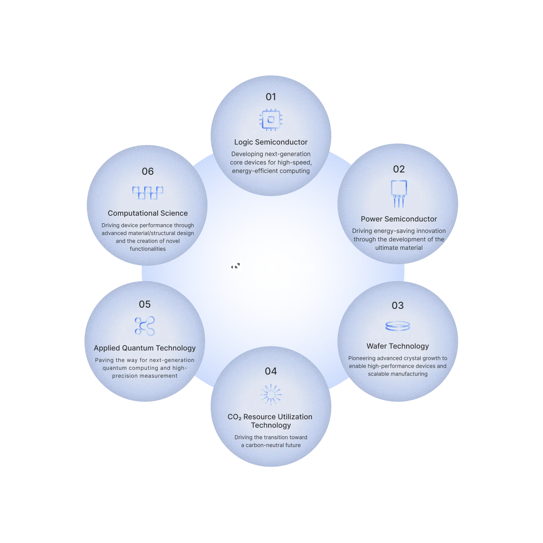
Organization: Under the leadership of Professor Tokuda—a renowned figure in the fields of diamond wafers, processing, and semiconductor, quantum, and energy devices—the center has established a robust structure consisting of six specialized research groups.
The Potential and Research Challenges of Diamond Semiconductors
Synthetic diamond possesses extraordinary potential that surpasses conventional silicon, thanks to its exceptional thermal conductivity and resilience against high temperatures, high voltages, and radiation. These characteristics are directly linked to the technologies required for power semiconductors, space exploration, nuclear energy, quantum technology, and a carbon-neutral society—fields where global research is accelerating rapidly.
Our center offers a rare research environment within Japan, providing a seamlessly integrated workflow—from material (wafer) development and processing to device application. We are tackling frontier themes such as diamond CMOS, logic devices, and CO2 recycling (resource recovery) technologies, pushing the boundaries of what is possible with diamond science.

The Story Behind the Logo
Connecting Kanazawa’s Light to the World, Illuminating the Future


Beacon Lantern
This logo is inspired by the Toro (traditional stone lantern), a symbol of Kanazawa, while also evoking the image of a transmission tower—a "hub" where research converges and radiates outward.
The "guiding light" and "unshakeable foundation" represented by the lantern embody ARCDia’s core values: reliability, cutting-edge innovation, and a commitment to illuminating the future through research.
Mizuhiki
The design incorporates the essence of Mizuhiki (traditional decorative cord), symbolizing the "tying and connecting" of research collaborations and our enduring dedication to continuous exploration.
Identity
The design integrates the letters "A," "R," and "C" of ARCDia with a diamond motif, reinforcing our core identity as an organization.
Guided by our research philosophy, "Exploring the Unknown, Creating the Future," our center accelerates interdisciplinary research in collaboration with industry partners and experts across diverse fields, including space, healthcare, and energy.
By integrating with industry-academia partnerships and regional semiconductor clusters, we strive to achieve "Innovating from Kanazawa, Leading the World". Our mission is to drive the early social implementation of these technologies, while powerfully advancing the creation of future semiconductor ecosystems and the cultivation of next-generation talent.
2035
2050
for Humanity.
2016-
2030
2016
Development of an
Inversion channel
Diamond MOSFET
Powered by proprietary technology
from Kanazawa
University
2025
10x Performance
Increase
2040
for human life in space.
2016-
2030
2016
Development of an
Inversion channel
Diamond MOSFET
Powered by proprietary technology
from Kanazawa
University
2025
10x Performance
Increase
2035
2040
for human life in space.
2050
for Humanity.