03
 Wafer Technology

| Group Leader: | Masayoshi Ichikawa, Ph.D. Specially Appointed Associate Professor |
|---|---|
| Specialization: |
|
| Keywords: |
|
Pioneering advanced crystal growth to enable high-performance devices and scalable manufacturing
Research Mission: Crystal Growth and Wafer Engineering
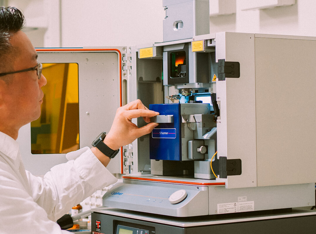
Breaking the Bottleneck: The Foundation for Social Implementation The performance and reliability of any semiconductor device are fundamentally dictated by the quality of the underlying wafer. While high-quality Silicon (Si) wafers are mass-produced through mature technology, the synthesis of large-diameter, low-defect single-crystal diamond remains a primary bottleneck due to the extreme difficulty of its growth. Breaking through this barrier is the most critical factor in bringing diamond semiconductors to practical social implementation.
Our group specializes in the manufacturing technology of high-quality single-crystal wafers, focusing on large-diameter scaling and the ultimate reduction of crystal defects. Our core strength lies in Kanazawa University’s long-standing expertise in process design and operational know-how, which enables high-speed growth while simultaneously suppressing defects.
Specific Research Themes
We are working toward the realization of inch-sized wafers tailored for power and logic devices, aerospace radiation sensors, and photoemission sources. In addition to advancing homoepitaxial growth, we leverage our academic strengths to develop innovative heteroepitaxial growth technologies. As wafers increase in size, controlling defect formation and lattice strain becomes exponentially more challenging. To overcome this, we integrate our proprietary growth systems with advanced nano-metrology for real-time defect analysis and feedback. Furthermore, we are tackling the precise control of high-purity growth and uniform dopant distribution to enhance overall device reliability.
Tailor-Made Wafer Technology
Different applications require different crystal specifications. We aim to establish "tailor-made" wafer manufacturing technology by controlling defect and impurity concentrations from the initial growth stage. Furthermore, we are systematizing the scientific understanding of how lattice defects impact device characteristics to create a comprehensive roadmap for wafer production.
By working in close collaboration with our device development groups, we rapidly translate functional requirements into process optimizations. We serve as the bridge between fundamental research and production-level wafer technology, supporting the early social implementation of next-generation semiconductors from the ground up.
 Group Members
Associate Professor
Kimiyoshi ICHIKAWA

Guest Professor
Christoph E. NEBEL